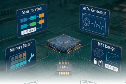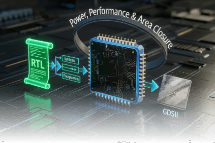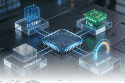
RTL Design & Development
Custom RTL design and development for complex digital systems using industry-standard HDLs.
- High-Performance RTL for Complex Digital Systems
- Expertise in Verilog / SystemVerilog / VHDL
- IP core design and seamless SoC integration
- Accelerated RTL simulation using Verilator for large-scale SoC validation
- Clock domain crossing (CDC) handling
- Low-power RTL techniques (UPF, MV design)
- Configurable and reusable IP libraries